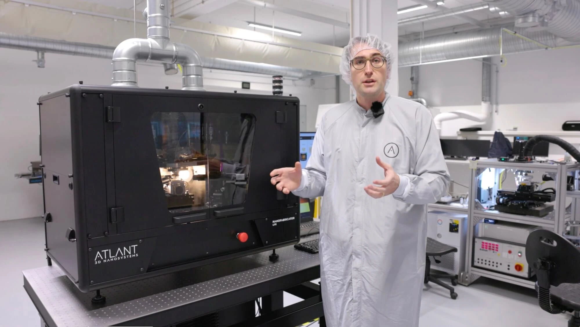
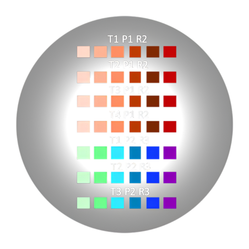
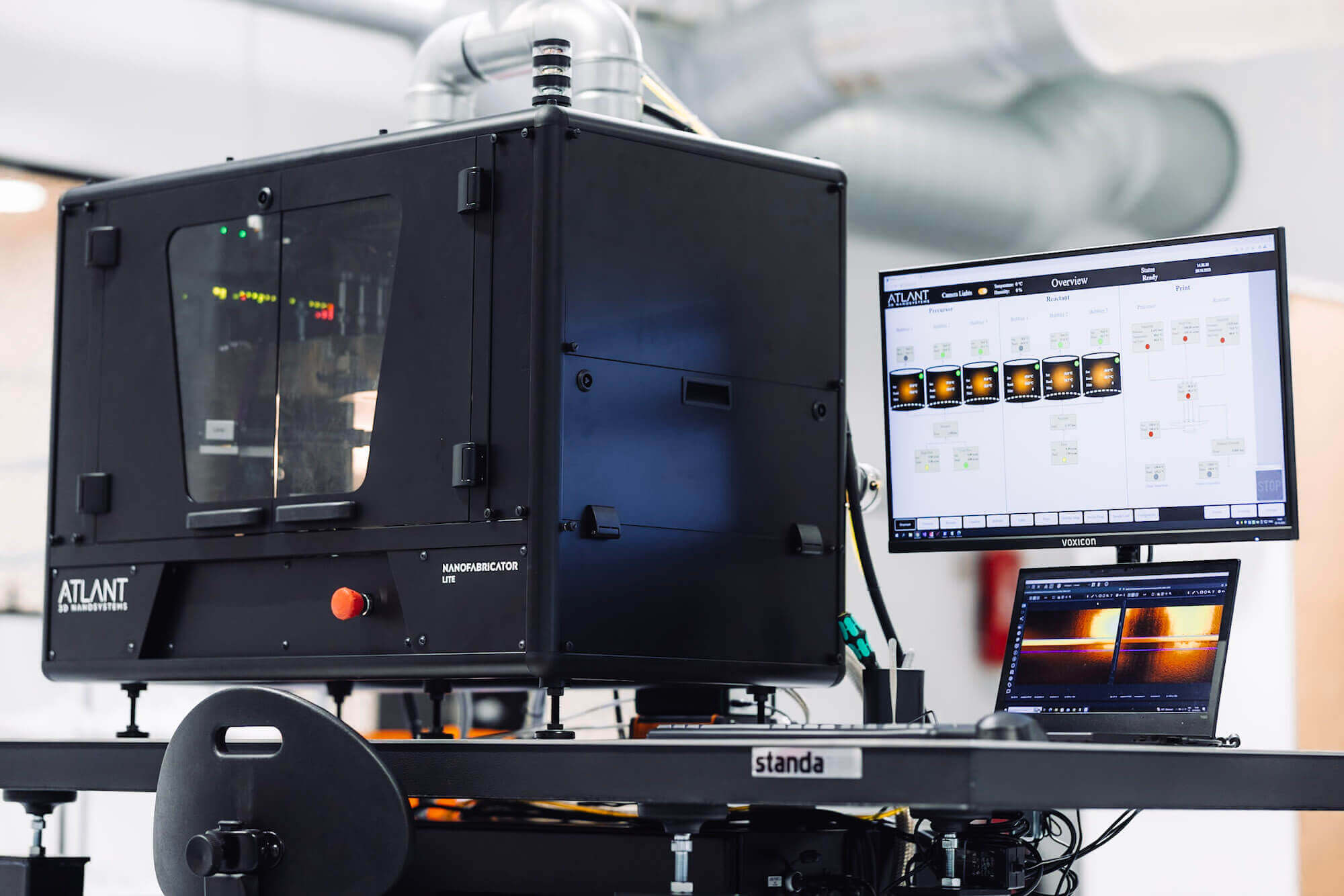
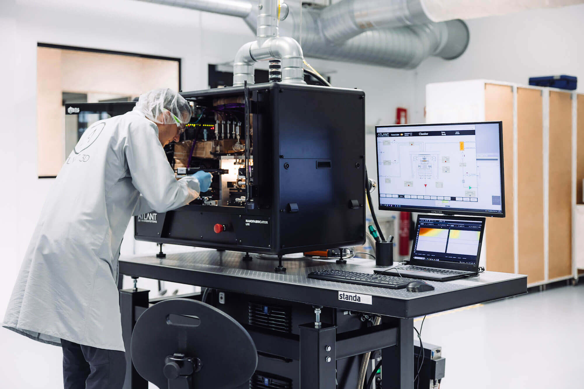
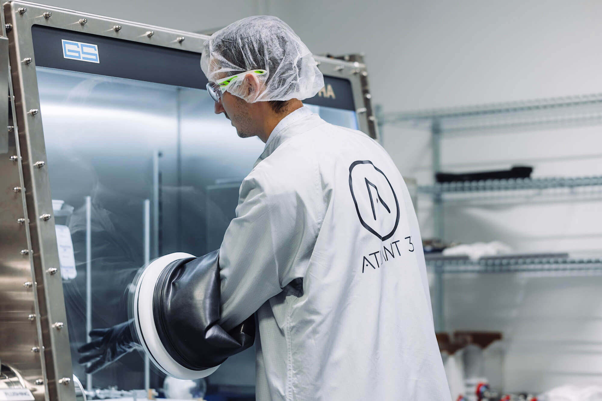
Discover the most versatile & powerful tool ever created to accelerate advanced material innovation, rapid process testing & device development with atomic precision. Experience the unprecedented flexibility & material versatility! We enable on-demand next-generation microdevices printing on simple and complex surfaces atom-by-atom. The NANOFABRICATOR™ LITE is the most compact tool ever created to accelerate materials, processes and device innovation with atomic precision. It is suitable for a wide range of applications such as MEMS, devices, optics, photonics, packaging, RF & electronics and quantum devices which can be developed with ATLANT 3D technology with previously impossible functionality and speed at a fraction of a cost. The whole process from experiment design to obtaining samples can take hours with several various DOE parameters. The processed sample has completed DOE with multiple parameter variations including thicknesses, temperatures, and materials. This step involves creating a detailed digital blueprint of the desired pattern. It requires precise design work to ensure that the specifications of the pattern are accurately represented and ready for processing. In this phase, a systematic approach is taken to plan the experiment. It includes defining the process parameters and conditions, setting up the necessary files, and ensuring that all variables are considered for a successful outcome. Here, a blank substrate is loaded into the NANOFABRICATOR™ LITE. This substrate serves as the base material on which the processing will be carried out, according to the predefined digital pattern and DOE parameters. This step signifies the completion of the processing phase. The substrate, now imprinted with the desired pattern through the Nanofabricator’s precise atomic layer processing, is ready for inspection and further use. This final stage involves the core technology of the NANOFABRICATOR™ LITE. It precisely adds or removes material at an atomic scale, following the digital pattern and DOE guidelines, to create the final micro- or nano-structured sample. The NANOFABRICATOR™ LITE enables advanced material innovation, rapid process testing, and device development across multiple advanced applications. It exemplifies a paradigm shift across diverse industrial landscapes. Explore how our cutting-edge equipment is advancing industries by offering precision, efficiency, and versatility in nanofabrication. DISCOVER APPLICATIONS * Dependent on materials to be deposited and customer needs. ** Additional number of bubblers and reactants dependent on customer needs. *** Additional reactant types dependent on customer needs. **** Clean room, CLASS 8 min recommended. ***** Argon recommended. NANOFABRICATOR™ LITE
![]() DALP® Technology
DALP® Technology REDEFINING MICROFABRICATION
![]() HOW WE DO IT
HOW WE DO IT SIMPLIFYING THE WHOLE PROCESS
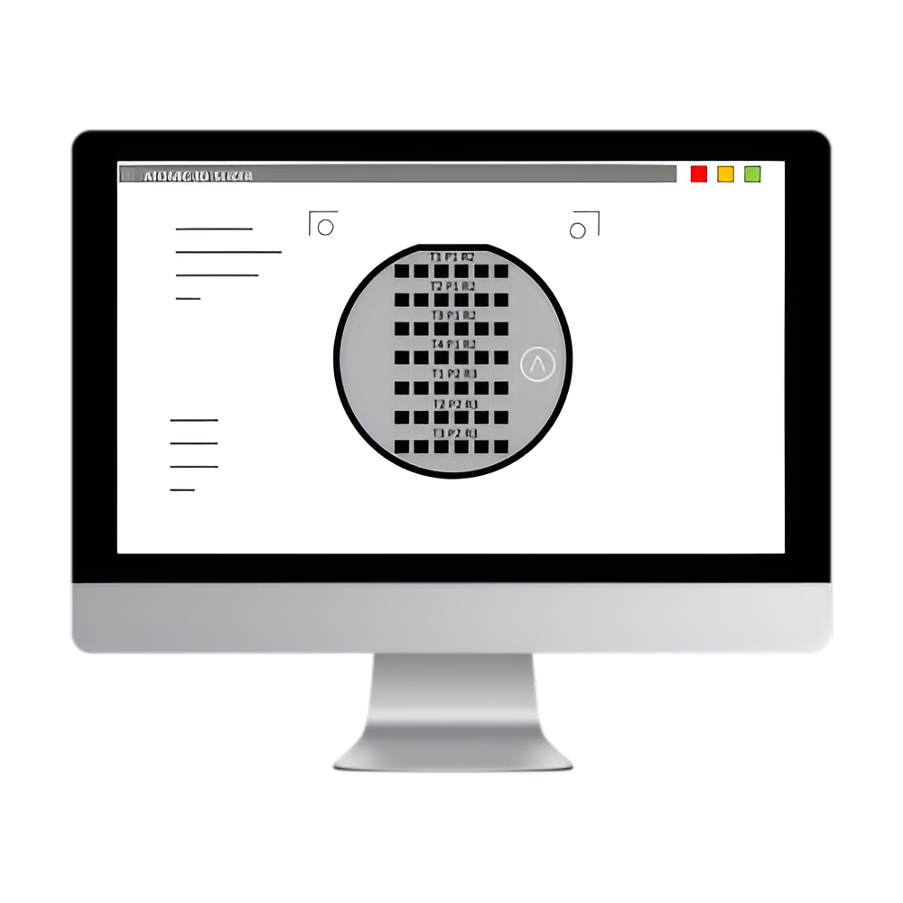
PREPARING DIGITAL PATTERN FILE
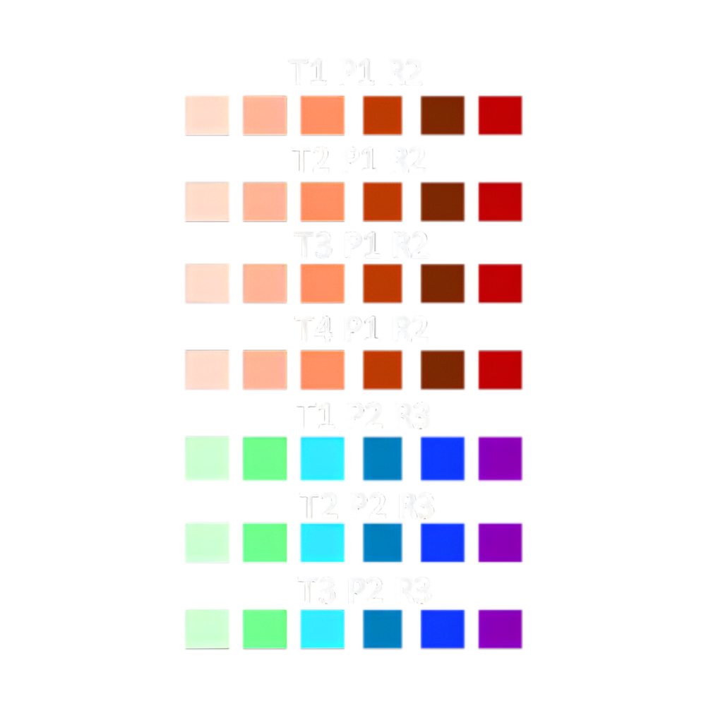
DEFINING DOE PROCESS FLOW AND FILES

UPLOADING BLANK SUBSTRATE
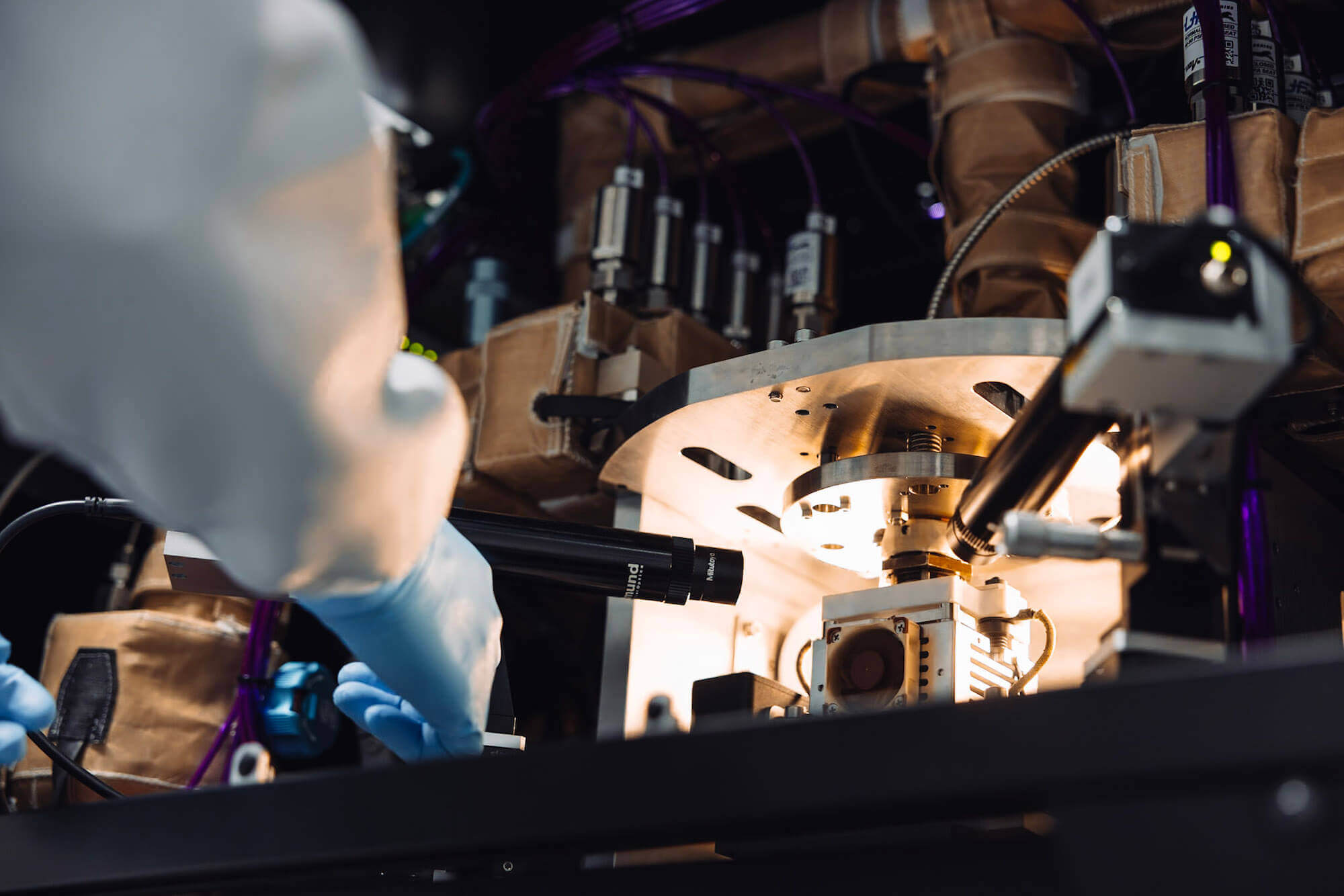
DIRECT ATOMIC LAYER PROCESSING
PROCESSED SAMPLE COMPLETED
![]() Expanding Horizons
Expanding Horizons Diverse Advanced Applications
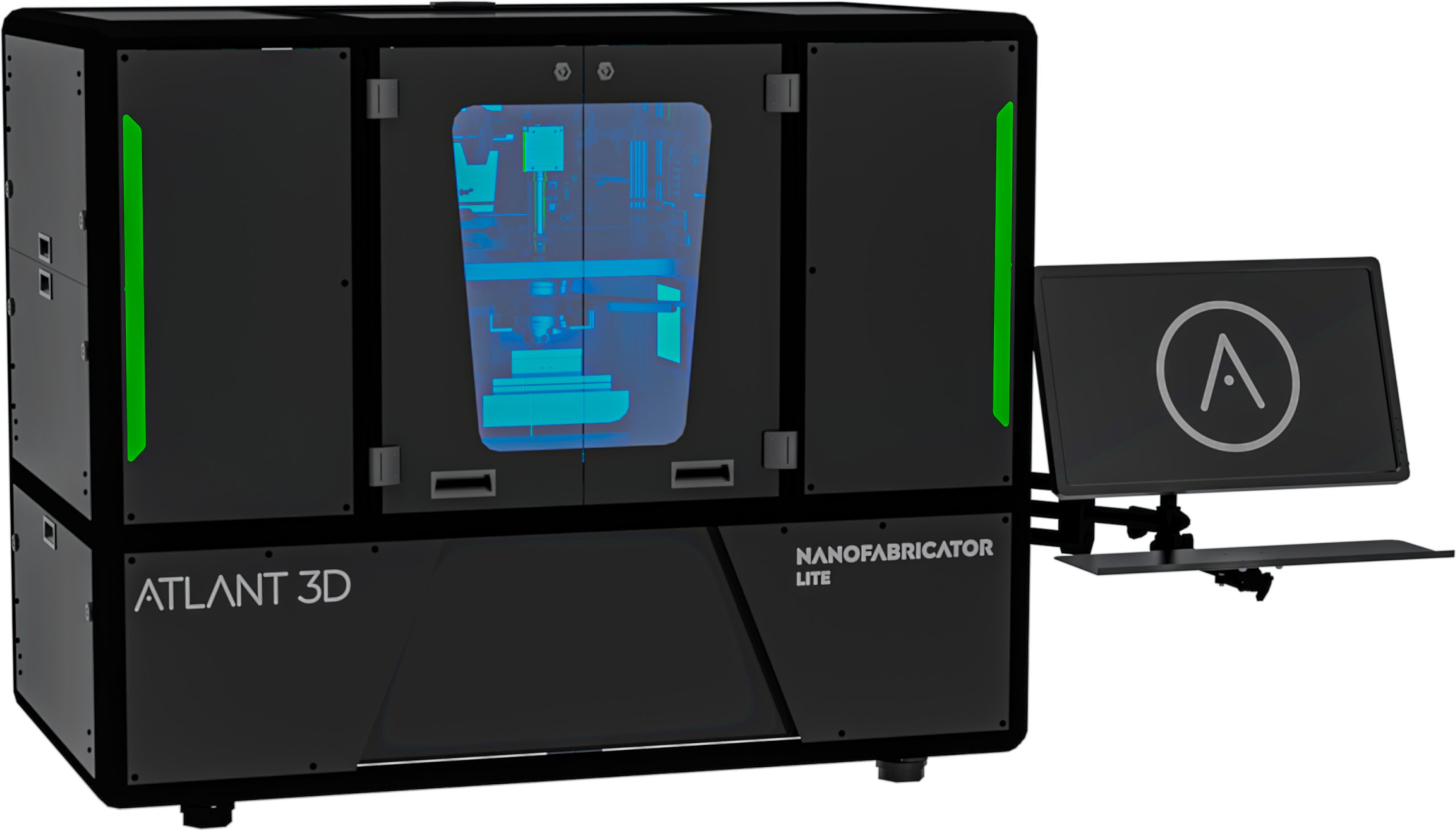
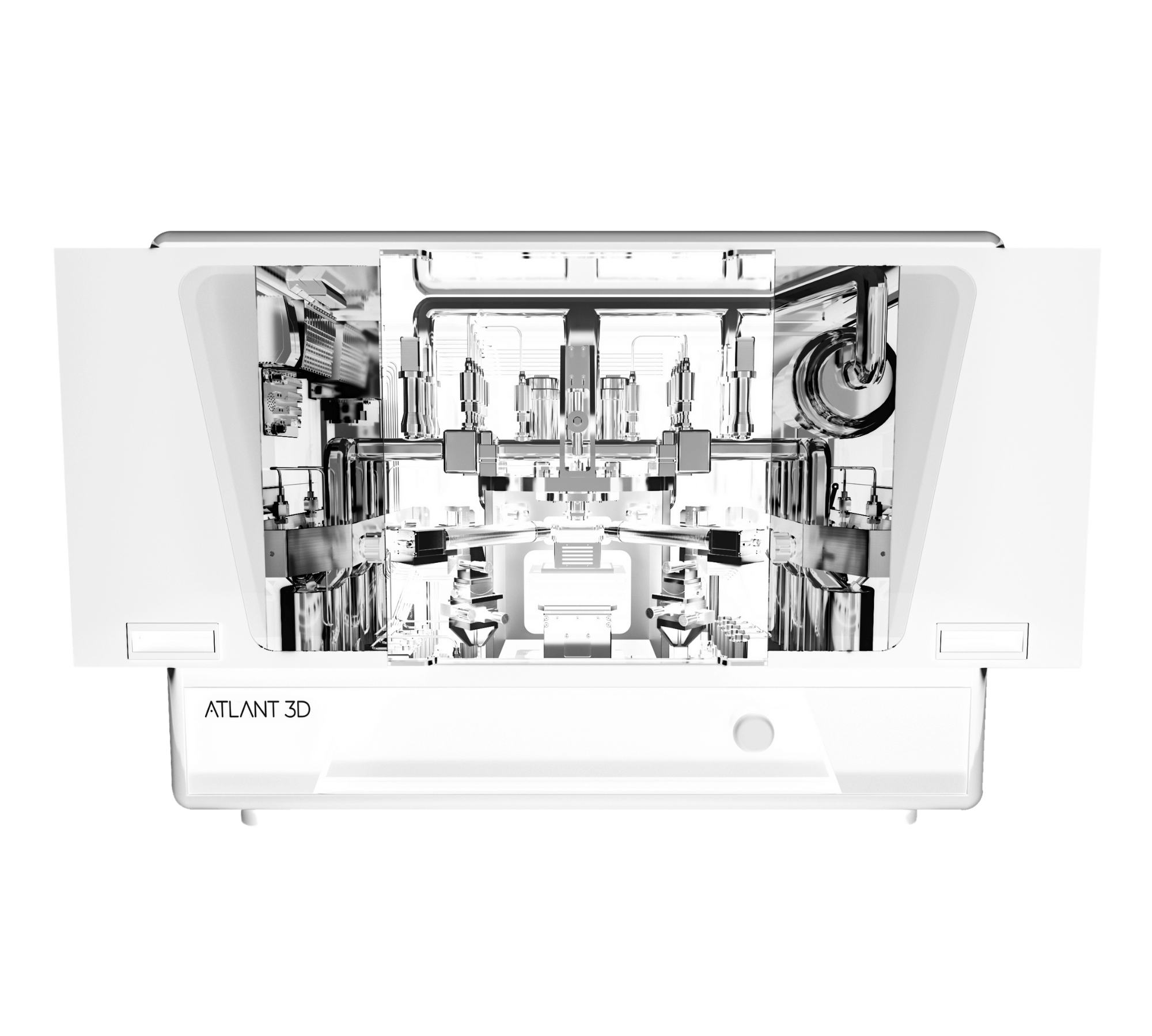
![]() Nanofabricator™ LITE
Nanofabricator™ LITE Technical Specification

Substrate
Process Chamber
Gas system
Options


Academia & Research
01
02
03
04
05